
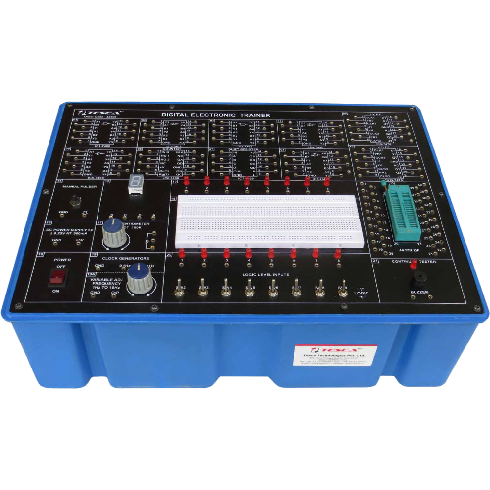
All in One Digital Electronics Experimental Station
Order Code: 23246922.3
Category: General Lab Equipment III
Body Material:Hard Round support board or Plastic Sheet Sheet Type: Digital Sheet thickness 6 mm Two-Part Combination(Transparent/white) UV Printout Protection System Feature: Safety tripping Low insertion loss and high reli...
SPECIFICATION
- Body Material:Hard Round support board or Plastic Sheet
- Sheet Type: Digital
- Sheet thickness 6 mm
- Two-Part Combination(Transparent/white)
- UV Printout
- Protection System
Feature:
- Safety tripping
- Low insertion loss and high reliability
- Panel Box
- Shape: Rectangular
- Surface Finish: Smooth
- High quality raw material
- Best structure
- Sheet thickness 5mm
- Sheet (Silver/white)
- Square Shape
- Power Supply
- Output Voltage 5VDC
- Output Current 10000 mA
- Power Nature
- Input Voltage (100-250)VAC
- Power Monitoring
- Self-operating voltage 5V
- Self-Consumption Current 2500 mA
- Power Nature
- Two-row for Voltage & Current
- Use Connector
- Banana Female Connector Diameter 4 mm
- Banana Male Connector Diame+ter 4 mm
Feature:
- Safety tripping
- Low insertion loss and high reliability
- Panel Box
- Shape: Rectangular
- Surface Finish: Smooth
- High quality raw material
- Best structure
- Sheet thickness 5mm
- Sheet (Silver/white)
- Square Shape
- Power Supply
- Output Voltage 5VDC
- Output Current 10000 mA
- Power Nature
- Input Voltage (100-250)VAC
- Power Monitoring
- Self-operating voltage 5V
- Self-Consumption Current 2500 mA
- Power Nature
- Two-row for Voltage & Current
- Use Connector:
- Banana Female Connector Diameter 4 mm
- Banana Male Connector Diame+ter 4 mm
- Working area:
- Working area: 35*24 inch
Experiment Block Feature:
- 10-line-to-4-line and 8-line-to-3-line priority encoders
- It operates at 4.5V to 5.5 DC voltage.
- It delivers output current from low 70µA to high 8mA
- It operates at the temperature from -55? to 70?
- 4Bit BCD to Decimal decode
- Applicable for: BCD to 7 Segment converters and displays number from 0 to 9.
- Maximum Voltage supply: 5.25V.
- Minimum Voltage supply: 4.75V.
- Package contains: checked and unused 1 piece of 7447 Ic.
- Type: DIP.
- 3-state outputs with common output ENABLE
- Separate SET and RESET inputs for each latch
- NOR and NAND configurations
- It is a Dual JK FF IC.
- Its operating speed is 16MHz.
- Its operating voltage is 5V/10V/15V.
- Its max operating voltage is 20v.
- Input Rise or Fall time at 5V is 45us.
- High Range i/p voltage min is 2V.
- The low-level i/p voltage max is 0.8V.
- Two J-K Master/Slave Flip Flops
- Outputs Directly Interface to CMOS, NMOS and TTL
- Large Operating Voltage Range
- Low ON resistance: 125 (typ.) over 15 Vp-p signal-input range for VDD - VSS = 15 V
- High OFF resistance: channel leakage of ±10 pA (typ.) @ VDD - VSS = 10 V
- Matched switch characteristics: RON = 5 (typ.) for VDD - VSS = 15 V
- Very low quiescent power dissipation under all digital-control input and supply conditions: 0.2 uW (typ.) @ VDD - VSS = 10 V
- Binary address decoding on chip
- 5-V, 10-V, and 15-V parametric ratings
- 100% tested for quiescent current at 20 V
- Maximum input current of 1 µA at 18 V over full package-temperature range; 100nA at 18 V and 25°C
- De-Multiplexer(74155): hardware details: To be mentioned by the bidder
- IC 74155 is a dual 1:4 line demultiplexer with individual strobe inputs.
- It has common binary address inputs (A, B and C) and it is available in single 16 pin package.
- To enable a section, we have to connect the corresponding strobe input to ground.
- When both the sections are enabled, the common binary address inputs (A, B, C) can be used to select the outputs of both sections.
- The data applied to input IC is inverted at its output and that applied at pin number 15 is not inverted through the output.
- The data on the input pins is clocked into the first register.
- All previously registered data will be shifted over to make room for the new input.
- Every cycle, data at the far end of the chain will be clocked out.
- 8-bit First-In-First-Out buffer queue in this regard.
- perating voltage ranges from 2V – 6V
- Clock frequency max is 25 MHz at 4.5V
- Power utilization is 80uA
- The sink current is 35mA
- Low-level input voltage Max: 1.35V
- High-level i/p voltage min 3.15V
- Max quiescent current is 80 µA
- Max input current is 1µA
- Shift frequency is DC-30 MHz
- High noise immunity.
- Wide Operating Voltage Range of 2 V to 6 V
- Outputs Can Drive Up to 10 LSTTL Loads
- Low Power Consumption, 80-µA Maximum ICC
- Typical tpd = 13 ns
- ±4-mA Output Drive at 5 V
- Low Input Current of 1 µA Maximum
- Complementary Outputs
- Direct Overriding Load (Data) Inputs
- Gated Clock Inputs
- Parallel-to-Serial Data Conversion
- An 8-bit, parallel-out serial-in Shift register
- Operating Voltage: 3V to 18V
- Supply Voltage - Max:5.25 V
- Propagation Delay Time: 25 ns
- Max. Clock Frequency: 36 MHz
- Operating Temperature Range: 0C to + 70 C
- Fully Buffered Clock
- Available in 16-pin PDIP, GDIP, PDSO packages
- Operating Voltage: 5V
- Supply Current: 23mA
- Supply frequency: 20MHz
- Parallel inputs and outputs
- Four operating modes:
- Synchronous parallel load Right shift Left shift
- Positive edge-triggered clocking
- Direct overriding clear
- Noise immunity is high, typically 0.45 VDD
- Operation is completely static
- TS or Storage Temperature ranges from −65°C to +150°C
- It has a 700 mW Power Dissipation, and its Dual-In-Line is
- The IC 4017 has a wide supply voltage range from 3V to 15V power.
- IC 4017 has well-matched compatibility with Transistor-Transistor Logic.
- IC 4017 has an operational speed or clock speed of 5 MHz.
- It provides a decoded tenten, output pin support system.
- CD40193 4-bit Up/Down Binary Counter IC
- Series: CD40193
- Function: Counter
- Product Category: Counter Shift Registers
- Counter Type: Binary
- Counting Sequence: UP, Down
- Number of Bits: 4 bit
- Mounting Style: Through Hole
- 7-Segment Display Driver(CD4026/7447):
- IC number: 7447
- Applicable for: BCD to 7 Segment converters and displays number from 0 to 9
- Maximum Voltage supply: 5.25V
- Minimum Voltage supply: 4.75V
- Package contains: checked and unused 1 piece of 7447 Ic
- Type: DIP
- Memory System(7489/74189):
Accessories:
- Experiment Manual: 01 Set
- Power Cord: 01 No
- Connecting Wire & Cable
- Complete 5 days Training Included
- User Manual or User Guide
- Protection:Under voltage, Supply overvoltage, Drive overload, Instantaneous Over current, short circuit, Ground fault, etc
- Working area: 35*24 inch
- Experiment Block Feature:
- Encoder(74147): hardware details: To be mentioned by the bidder
- 10-line-to-4-line and 8-line-to-3-line priority encoders
- It operates at 4.5V to 5.5 DC voltage.
- It delivers output current from low 70µA to high 8mA
- It operates at the temperature from -55? to 70?
- 4Bit BCD to Decimal decode
- Applicable for: BCD to 7 Segment converters and displays number from 0 to 9.
- Maximum Voltage supply: 5.25V.
- Minimum Voltage supply: 4.75V.
- Package contains: checked and unused 1 piece of 7447 Ic.
- Type: DIP.
- 3-state outputs with common output ENABLE
- Separate SET and RESET inputs for each latch
- NOR and NAND configurations
- JK (4027):
- It is a Dual JK FF IC.
- Its operating speed is 16MHz.
- Its operating voltage is 5V/10V/15V.
- Its max operating voltage is 20v.
- Input Rise or Fall time at 5V is 45us.
- High Range i/p voltage min is 2V.
- The low-level i/p voltage max is 0.8V.
- JK Master/Slave(4073): hardware details: To be mentioned by the bidder
- Two J-K Master/Slave Flip Flops
- Outputs Directly Interface to CMOS, NMOS and TTL
- Large Operating Voltage Range
- Low ON resistance: 125 (typ.) over 15 Vp-p signal-input range for VDD - VSS = 15 V
- High OFF resistance: channel leakage of ±10 pA (typ.) @ VDD - VSS = 10 V
- Matched switch characteristics: RON = 5 (typ.) for VDD - VSS = 15 V
- Very low quiescent power dissipation under all digital-control input and supply conditions: 0.2 uW (typ.) @ VDD - VSS = 10 V
- Binary address decoding on chip
- 5-V, 10-V, and 15-V parametric ratings
- 100% tested for quiescent current at 20 V
- Maximum input current of 1 µA at 18 V over full package-temperature range; 100nA at 18 V and 25°C
- De-Multiplexer(74155): hardware details: To be mentioned by the bidder
- IC 74155 is a dual 1:4 line demultiplexer with individual strobe inputs.
- It has common binary address inputs (A, B and C) and it is available in single 16 pin package.
- To enable a section, we have to connect the corresponding strobe input to ground.
- When both the sections are enabled, the common binary address inputs (A, B, C) can be used to select the outputs of both sections.
- The data applied to input IC is inverted at its output and that applied at pin number 15 is not inverted through the output.
- The data on the input pins is clocked into the first register.
- All previously registered data will be shifted over to make room for the new input.
- Every cycle, data at the far end of the chain will be clocked out.
- 8-bit First-In-First-Out buffer queue in this regard.
- Operating voltage ranges from 2V – 6V
- Clock frequency max is 25 MHz at 4.5V
- Power utilization is 80uA
- The sink current is 35mA
- Low-level input voltage Max: 1.35V
- High-level i/p voltage min 3.15V
- Max quiescent current is 80 µA
- Max input current is 1µA
- Shift frequency is DC-30 MHz
- High noise immunity.
- Wide Operating Voltage Range of 2 V to 6 V
- Outputs Can Drive Up to 10 LSTTL Loads
- Low Power Consumption, 80-µA Maximum ICC
- Typical tpd = 13 ns
- ±4-mA Output Drive at 5 V
- Low Input Current of 1 µA Maximum
- Complementary Outputs
- Direct Overriding Load (Data) Inputs
- Gated Clock Inputs
- Parallel-to-Serial Data Conversion
- An 8-bit, parallel-out serial-in Shift register
- Operating Voltage: 3V to 18V
- Supply Voltage - Max:5.25 V
- Propagation Delay Time: 25 ns
- Max. Clock Frequency: 36 MHz
- Operating Temperature Range: 0C to + 70 C
- Fully Buffered Clock
- Available in 16-pin PDIP, GDIP, PDSO packages
- Universal(74LS194):
- Operating Voltage: 5V
- Supply Current: 23mA
- Supply frequency: 20MHz
- Parallel inputs and outputs
- Four operating modes:
- Synchronous parallel load Right shift Left shift
- Positive edge-triggered clocking
- Direct overriding clear
- Noise immunity is high, typically 0.45 VDD
- Operation is completely static
- TS or Storage Temperature ranges from −65°C to +150°C
- It has a 700 mW Power Dissipation, and its Dual-In-Line is
- The IC 4017 has a wide supply voltage range from 3V to 15V power.
- IC 4017 has well-matched compatibility with Transistor-Transistor Logic.
- IC 4017 has an operational speed or clock speed of 5 MHz.
- It provides a decoded tenten, output pin support system.
- CD40193 4-bit Up/Down Binary Counter IC
- Series: CD40193
- Function: Counter
- Product Category: Counter Shift Registers
- Counter Type: Binary
- Counting Sequence: UP, Down
- Number of Bits: 4 bit
- Mounting Style: Through Hole
- 7-Segment Display Driver(CD4026/7447):
- IC number: 7447
- Applicable for: BCD to 7 Segment converters and displays number from 0 to 9
- Maximum Voltage supply: 5.25V
- Minimum Voltage supply: 4.75V
- Package contains: checked and unused 1 piece of 7447 Ic
- Type: DIP
- Memory System(7489/74189):
Enquiry Form
Related Product


Tesca specialize in doing turnkey projects that is fully operable when it is handed over to the project authority. Starting from inception to application training, Tesca provides the services as ONE source solution. Working side by side with government authorities and people across the World, we help countries to perform better. We support countries grow their economies, strengthen their education and health systems and improve financial management. We do this by providing consultancy & training in environment safety, education, health strengthening.
Category
Useful Links
Contact Us
International Sales:
 91-9829132777
91-9413330765
India Sales:
91-9588842361
2026 © All Rights Reserved.