
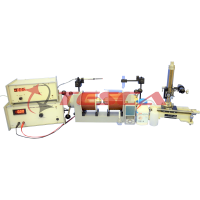
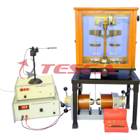
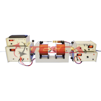
Study of Thermoluminescence of F-centres in Alkali Halide Crystals
Order Code: 55536
Category: Physics Trainers
Pure alkali halide crystals are transparent throughout the visible region of the spectrum. The crystals may be colored in a number of ways by the introduction of chemical impurities by introducing an excess of the metal ion by X-ray, g-ray,...
SPECIFICATION
- by the introduction of chemical impurities
- by introducing an excess of the metal ion
- by X-ray, g-ray, neutron and electron bombardment
- by electrolysis
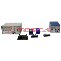
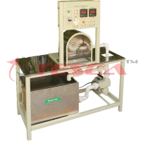
- Sample: KBr or KCl single crystal
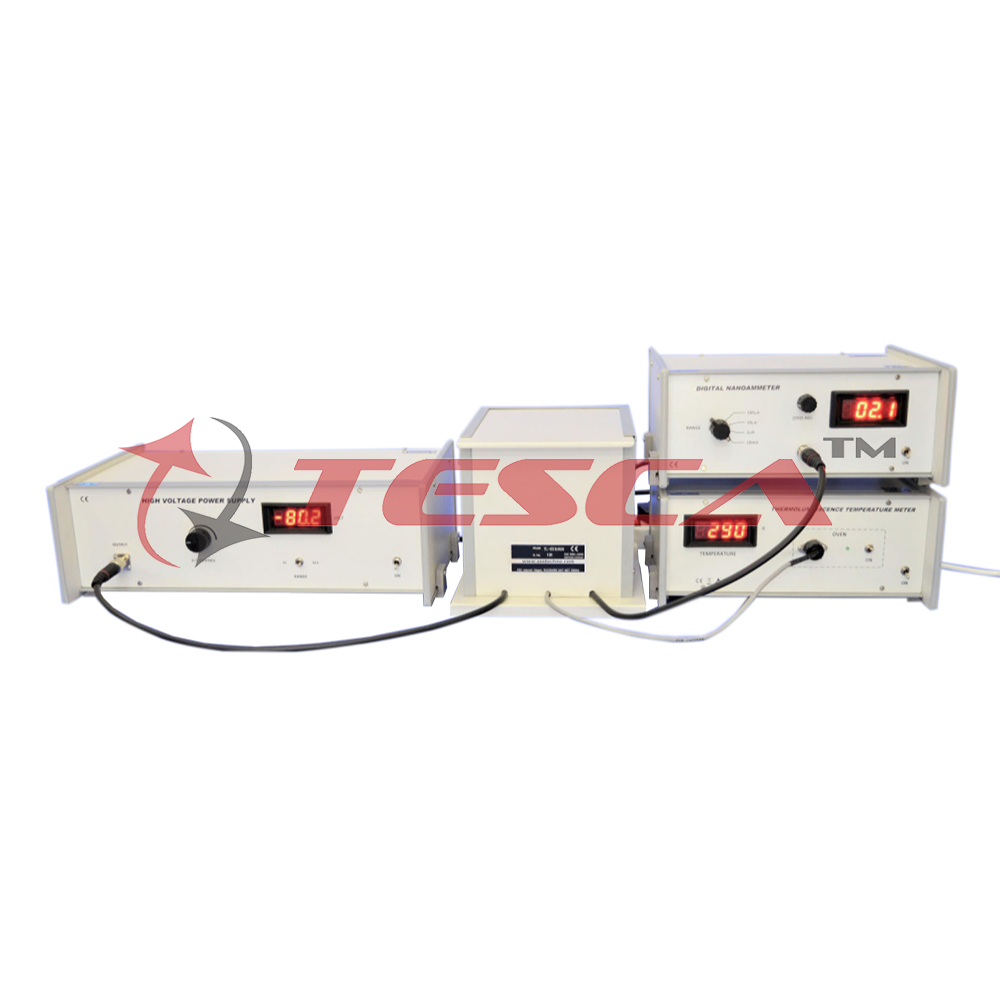
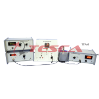
- Thermolumniscence Temperature Meter
- Digital Thermometer
- Oven Power Supply
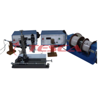
- Sample Holder
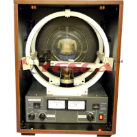
- Thermoluniscence Oven (0-423K)
- Black Box
- Photomultiplier tube: R11558
- PMT Housing with biasing circuit and coaxial cables etc.
- High Voltage Power Supply, Model: EHT-11
- Output : 0-1500V variable (1mA max.)
- Regulation : 0.05%
- Display : 3½ digit 7-segment LED
- Nanoammeter, Model DNM-121
- Range : 100nA to 100mA full scale in 4 ranges
- Accuracy : 0.2%.
- Display : 3½ digit 7-segment LED
- Spectral Response
- Range : 300 to 650(nm)
- Peak wave length : 400nm
- Photo Cathode Material : Bialkali
- Dynode Structure/No. of Stages : CC/9
- Maximum Cathode Voltage : 1250Vdc
- Maximum Average Anode Current : 0.1mA
- Cathode Sensitivity
- Minimum : 40µA/lm
- Typical : 60µA/lm
- Anode Sensitivity
- Minimum : 200A/lm
- Typical : 600A/lm
- Anode to Cathode
- Supply Voltage : 1000Vdc
- Current Amplification : 1.0x10⁷
- Anode Dark Current (after 30min)
- Typical : 1nA
- Maximum : 10nA
Enquiry Form
Related Product
Tesca specialize in doing turnkey projects that is fully operable when it is handed over to the project authority. Starting from inception to application training, Tesca provides the services as ONE source solution. Working side by side with government authorities and people across the World, we help countries to perform better. We support countries grow their economies, strengthen their education and health systems and improve financial management. We do this by providing consultancy & training in environment safety, education, health strengthening.
Category
Useful Links
Contact Us
International Sales:
 91-9829132777
91-9413330765
India Sales:
91-9588842361
2026 © All Rights Reserved.