Experimental Determination of :
- Reverse saturation current I0 and material constant h
- Temperature coefficient of junction voltage dV/dt
- Energy band-gap Vg0
- Junction capacitance
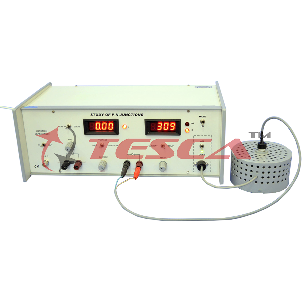
This is an advanced level experiment to be performed on commercially available diodes viz. germanium or silicon diodes, various types of LED’s and also on the base - emitter/collector-base junctions of a transistor. The results of the experiments not only give the device characteristics but also provide an insight into the properties of the materials used in the fabrication of the junction. In the set-up, all the necessary instrumentation is integrated as a result of which a minimum of external connections need to be made by the user. A CRO is the only accessory that is required.
Experiments
Given below is a brief description of the experiments that may be performed.
(a) Reverse saturation current I0 and material constant h
The magnitude of I0 is too small to be measured conveniently and further, it is a function of the applied voltage. The direct measurement of this current is therefore both difficult and erroneous. In the present set-up, readings for the forward V-I characteristics are obtained by 3½ digit DPM for a wide range of currents. If, V and lnI are plotted on a graph paper a straight line is obtained. This line intersects the current (lnI) axis at lnI0 and its slope DV/DlnI may be solved to compute h. (fig.1)
Experimental Determination of :
- Reverse saturation current I0 and material constant h
- Temperature coefficient of junction voltage dV/dt
- Energy band-gap Vg0
- Junction capacitance
This is an advanced level experiment to be performed on commercially available diodes viz. germanium or silicon diodes, various types of LED’s and also on the base - emitter/collector-base junctions of a transistor. The results of the experiments not only give the device characteristics but also provide an insight into the properties of the materials used in the fabrication of the junction. In the set-up, all the necessary instrumentation is integrated as a result of which a minimum of external connections need to be made by the user. A CRO is the only accessory that is required.
Experiments
Given below is a brief description of the experiments that may be performed.
(a) Reverse saturation current I0 and material constant h
The magnitude of I0 is too small to be measured conveniently and further, it is a function of the applied voltage. The direct measurement of this current is therefore both difficult and erroneous. In the present set-up, readings for the forward V-I characteristics are obtained by 3½ digit DPM for a wide range of currents. If, V and lnI are plotted on a graph paper a straight line is obtained. This line intersects the current (lnI) axis at lnI0 and its slope DV/DlnI may be solved to compute h. (fig.1)
(b) Energy band-gap and temperature coefficient of the junction voltage
The P-N junction under test is kept in as small, fast temperature controlled oven. The temperature is adjustable in the range from room temperature to about 80°C. From the readings of the temperature and junction voltage on digital instruments provided on the panel, the temperature coefficient and energy band-gap are computed. (fig.2)
(C) The Junction Capacitance
The junction capacitance of a typical diode varies in the range 10pf-100pf approximately, as a non-linear function of the reverse voltage. This parameter though important in high frequency circuits, is difficult to measure because of its small value. In the present set-up, the output V1 and V2 at two frequencies f1 & f2, where f2>f1, are obtained at different values of bias voltage to compute the junction capacitance. A typical graph between bias voltage and junction capacitance is shown in fig.3.
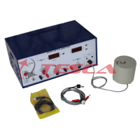
The experimental set-up consists of the following
(1) Study of P-N Junction - 55541
- 3½ digit DPM for current/temperature measurements.
- 3½ digit DPM for bias voltage/junction voltage measurements.
- Two parts to connect the diode - one for experiment 1 & 2 and other for experiment 3.
- Two fixed frequency oscillators (5KHz & 20KHz) with the same output (200 mV).
(2) Fast temperature controlled oven with sensor
(3) Set of samples
- Transistor BC109 (base-emitter)-Si
- Transistor AC126 (base-emitter)-Ge
- Diode 1N 5408/1N 4007-Si
The unit is supplied complete with a detailed instruction manual. Sufficient theoretical description is included for a proper understanding. This is followed by a step-by-step procedure and a typical set of readings and results.
Complete in all respect, except a CRO for capacitance measurement. Typical results obtained are shown in fig. no. 1, 2 & 3.
(b) Energy band-gap and temperature coefficient of the junction voltage
The P-N junction under test is kept in as small, fast temperature controlled oven. The temperature is adjustable in the range from room temperature to about 80°C. From the readings of the temperature and junction voltage on digital instruments provided on the panel, the temperature coefficient and energy band-gap are computed. (fig.2)
(c) The Junction Capacitance
The junction capacitance of a typical diode varies in the range 10pf-100pf approximately, as a non-linear function of the reverse voltage. This parameter though important in high frequency circuits, is difficult to measure because of its small value. In the present set-up, the output V1 and V2 at two frequencies f1 & f2, where f2>f1, are obtained at different values of bias voltage to compute the junction capacitance. A typical graph between bias voltage and junction capacitance is shown in fig.3.


 91-9829132777